Junction isolated (JI) Gate Driver ICs
JI Level Shift High Voltage Gate Driver ICs for IGBTs and MOSFETs

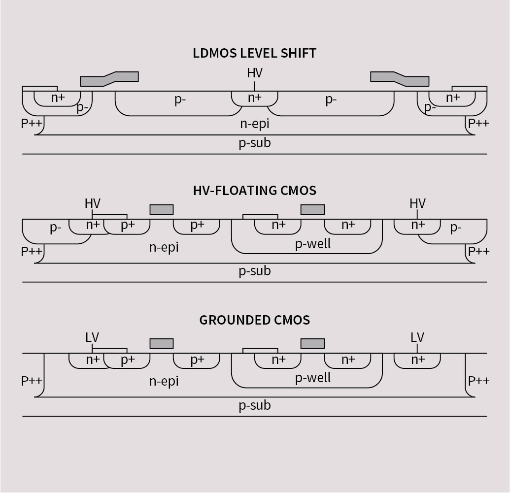
The p-n junction-isolation (JI) technology is a mature, proven industry-standard MOS/CMOS fabrication technique. Our proprietary high-voltage integrated circuit (HVIC) and latch-immune CMOS technologies enable rugged monolithic construction. The advanced process allows monolithic high-voltage and low-voltage circuitry construction with the best price per performance for specific motor-control and switch-mode power applications.
The JI Level Shift High Voltage Gate Driver ICs family provide advanced features such as over current protection, shutdown, fault reporting, enable, OPAMP, DESAT, programmable deadtime, shoot through protection, separate sink and source outputs, low UVLO (5 V), self-oscillating, etc.
We offer industrial and automotive-qualified Junction isolated (JI) gate driver ICs.
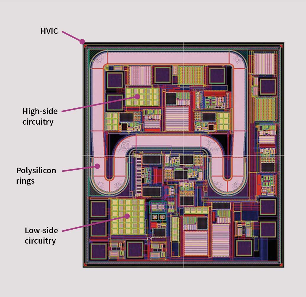
Pioneered by International Rectifier (IR) since 1989 with the introduction of the first monolithic product, the high-voltage integrated circuit (HVIC) technology uses patented and proprietary monolithic structures integrating bipolar, CMOS, and lateral DMOS devices with breakdown voltages above 700 V and 1400 V for operating offset voltages of 600 V and 1200 V.
Using this mixed-signal HVIC technology, both high-voltage level-shifting circuits and low-voltage analog and digital circuits can be implemented. With the ability to place high-voltage circuitry (in a ‘well’ formed by polysilicon rings) , that can ‘float’ 600 V or 1200 V, on the same silicon away from the rest of the low-voltage circuitry, high-side power MOSFETs or IGBTs exist in many popular off-line circuit topologies such as buck, synchronous boost, half-bridge, full-bridge and three-phase.
These HVIC gate drivers with floating switches are well-suited for topologies requiring high-side, half-bridge, and three-phase configurations.
This might also be of interest for you
Recommended documents
You will have a glimpse of the different gate driver technologies available at Infineon and their benefits.
For a better understanding we will take a look at the optimization of external gate resistors to drive MOSFETs in a given application.
With this training, you will learn how to calculate a gate resistance value for an IGBT application, how to identify suitable gate driver ICs based on peak current and power dissipation requirements, and how to fine-tune the gate resistance value in laboratory environment based on worst case conditions.
We offer a large portfolio of level shift high voltage gate drivers – silicon-on-insulator (SOI) and junction isolated (JI) technologies. Learn about the advantages of Infineon SOI gate driver: integrated bootstrap diode, Low level-shift losses, saving space and cost, and negative VS robustness.


