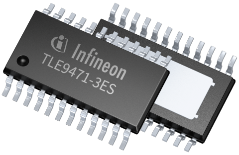
TLE9471-3ES
The TLE9471-3ES is a monolithically integrated circuit in an exposed pad PG-TSDSO-24-1 (150 mil) power package. The device is designed for various CAN automotive applications as main supply for the microcontroller and as interface for a CAN bus network including the CAN Partial Networking feature. To support these applications, the System Basis Chip (SBC) provides the main functions, such as a 5 V lowdropout voltage regulator (Buck SMPS) for e.g. a microcontroller supply, another 5 V low-dropout voltage regulator with off-board protection for e.g. sensor supply, a HS-CAN transceiver supporting CAN FD and CAN Partial Networking (incl. FD tolerant mode) for data transmission, a high-voltage GPIO with embedded protective functions and a 16-bit Serial Peripheral Interface (SPI) to control and monitor the device. Also implemented are a configurable timeout / window watchdog circuit with a reset feature, one Fail Output and an undervoltage reset feature. The device offers low-power modes in order to minimize current consumption on applications that are connected permanently to the battery. A wake-up from the low-power mode is possible via a message on the buses, via the bi-level sensitive monitoring/wake-up input as well as via cyclic wake.
Zusammenfassung der Merkmale
• Very low quiescent current consumption in Stop- and Sleep Mode
• Periodic Cyclic Wake in SBC Normal-, Stop- and Sleep Mode
• Periodic Cyclic Sense in SBC Normal-, Stop- and Sleep Mode
• Low-Drop Buck DC/DC Voltage Regulator 5 V, 500 mA for main supply with integrated spread spectrum modulation feature for optimum EMC performance
• Low-Drop Linear Voltage Regulator 5 V, 100 mA, protected features for off-board usage
• High-Speed CAN transceiver supporting FD communication up to 5 Mbit/s and featuring CAN Partial Networking & CAN FD tolerant mode according to ISO 11898-2:2016 & SAE J2284
• Fully compliant to “Hardware Requirements for LIN, CAN and FlexRay Interfaces in Automotive Applications” Revision 1.3, 2012-05-04
• Charge pump-Output for N-channel MOSFET reverse-polarity protection with integrated spread spectrum modulation feature for optimum EMC performance
• Universal High-Voltage Wake Input for voltage level monitoring and wake detection
• General Purpose High-Voltage In- and Output (GPIO) configurable as Fail Output, Wake Input, Low-Side switch or High-Side switch
• HIgh-Voltage Measurement Function as alternate pin assignment
• Fail Outputs for Fail-Safe signalization
• Configurable wake-up sources
• Reset Output & Interrupt Output
• Configurable timeout and window watchdog
• Overtemperature and short circuit protection feature
• Dedicated TEST pin for SBC Development Mode entry (watchdog counter stopped)
• Software compatible to all SBC families TLE926x and TLE927x
• Wide supply input voltage and temperature range
• Optimized for Electromagnetic Compatibility (EMC) and low Electromagnetic Emission (EME)
• Optimized for high immunity against Electromagnetic Interference (EMI)
• AEC Qualified & Green Product (RoHS compliant)
Potentielle Zielanwendungen
• In-Cabin Wireless Charger
• Transmission, Transfer Case, Gear shifter and selectors
• Exhaust module and NOx sensor
• In-Cabin Wireless Charger
• Water pump
• Wiper
• HVAC ECU and Control panel
• Light Control Unit (LCU) for front, rear and ambient
• Seat belt pretension
• Steering column and steering lock


