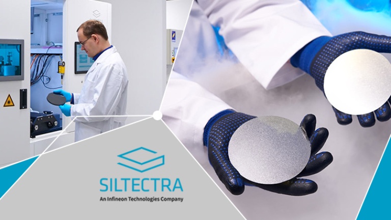
The SILTECTRA™ cold split technology splits crystalline materials with minimal loss of material compared to common sawing technologies. SILTECTRA™ technology can also be applied with the semiconductor material Silicon Carbide (SiC), for which rapidly rising demand is expected in the coming years. SiC products, such as Infineon CoolSiC™ devices are already used today in very efficient and compact solar inverters. In the future, SiC will play a more and more important role in electro-mobility.
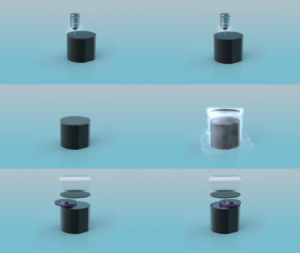
The laser-based technique employs a chemical-physical process that uses thermal stress to generate a force that splits the material with exquisite precision along the desired plane, and produces virtually no kerf loss. The “no kerf loss” capability is unique to cold split and delivers breakthrough advantages. First, it extracts more wafers per boule than conventional wafering technologies. This drives up output. Second, it dramatically reduces consumables costs.


