Power Block
Dual MOSFET solutions for superior power density
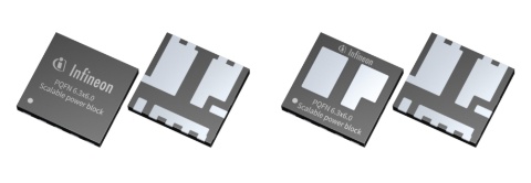
The power block package concept consists of integrating both the control and synchronous MOSFETs within the package. This enables replacing Q1/Q2 FETs in half-bridge configuration normally using two discrete MOSFETs solutions with a single package for superior power density, very low parasitics and higher efficiencies. They can be used in all applications that require half-bridge configuration like drives, SMPS etc.

OptiMOS™ 6 40 V & OptiMOS™ 5 100 V Symmetric power block (Q1 & Q2 of similar RDS(on)) integrates a low-side and a high-side MOSFET in a compact leadless SMD 6.3x6.0 mm² package targeting a variety of applications (drives, SMPS). By replacing two separate discrete packages, ex: SuperSO8 (PQFN 5x6), customers can shrink the power section on the board by at least 50%.
High performance and high current handling
The MOSFET half-bridge family features Infineon’s proven OptiMOS™ 5 & 6 technologies, offering very low on-state resistance (RDS(on)) and figure of merits (Qg, Qgd).
The reduction in the parasitic inductance of the package results in improved switching performance & EMI, as well as reduced overall BOM cost.
Optimized lead-frame and Cu-clip significantly improves thermal performance of the package. The dual-side cooling version of the package boosts the power throughput by an additional 25%.
| Key features | Key benefits | Potential applications |
|
|

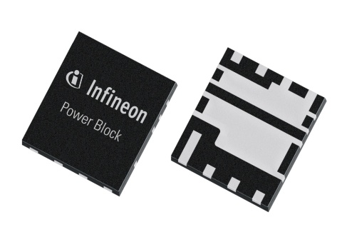
OptiMOS™ 5 power block is a leadless SMD 5.0x6.0 mm² small outline package, integrating a low-side and a high-side MOSFET targeting synchronous rectification buck converter applications. By replacing two separate discrete packages, such as SO8 or SuperSO8, with the space-saving MOSFET package, OptiMOS™ 5 power block 5x6 customers can shrink their designs by at least 50%. Standardizing power packages benefits the customer, as the number of different package outlines available on the marketplace is minimized.
Benchmark efficiency and high current handling
The MOSFET half-bridge family features Infineon’s proven OptiMOS™ 5 technology, which offers low on-state resistance (RDS(on)) and figure of merits (Qg, Qgd). The source-down connection of the low-side MOSFET results in a big PGND pad which significantly improves the thermal junction to the board, simplifying the layout and reducing EMI. This solution allows engineers to optimize their designs by increasing switching frequency and power density as well as reducing overall BOM costs.
| Key features | Key benefits | Potential applications |
|
|


