CoolSiC™ technology details
Unmatched reliability and quality
Our overall goal is to combine the low RDS(on) offered by silicon carbide MOSFETs with an gate drive mode in which the device operates in the safe oxide field-strength conditions. Consequently, it was decided to focus on trench-based devices moving away from a planar surface with high-defect density towards more favorable surface orientations. The latter enabling a low channel resistance at low oxide fields. These boundary conditions are the baseline for transferring quality assurance methodologies established in the silicon power semiconductor world in order to guarantee FIT rates expected in industrial and even automotive applications.
SiC devices operate at much higher drain-induced electric fields in the blocking mode compared to their Si counterparts (MV instead of kV). Thus, high electric fields in the oxide in the on-state AND off state can potentially accelerate the wear-out. For off state stress protection by deep p-regions is adopted, for on-state a thick oxide is used in order to circumvent the limits to screen remaining extrinsic oxide defects for thin oxides.

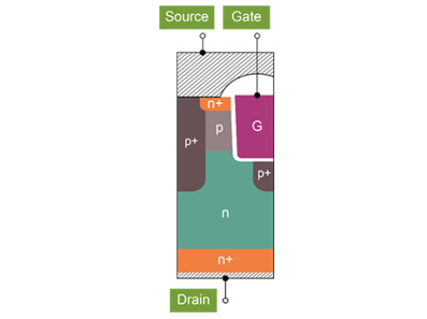
CoolSiC™ MOSFET cell structure

The CoolSiC™ MOSFET trench concept is optimized for the operation of the body diode. The trench bottom embedded into a p+ region enhances the body diode area.
The CoolSiC™ MOSFET cell design was developed to limit the electric field in the gate oxide in on-state as well as in off-state to maintain reliability. Additionally, for all variants a low on-resistance, stable and reproducible even in mass production, is achieved. Guaranteed at driving voltage levels of only VGS= 15 V combined with a sufficiently high gate-source-threshold voltage of typically 4.5 V, being a benchmark in the field of SiC transistors.
More about CoolSiC™ MOSFET

CoolSiC™ is synonymous with pioneering in trench SiC MOSFET technology. Infineon once again demonstrates that we continue to strive for innovation and technology leadership – also in the WBG arena. What we offer and the way we offer it, differentiates us.
The CoolSiC™ MOSFET features superior performance in terms of switching behavior and total losses. One of the highlights is the possibility to turn off the device with zero gate bias, which makes the CoolSiC™ transistor concept the only true “normally-off” device in the market at the moment.
In addition to superior gate oxide reliability and a stable, robust body diode is a key feature of CoolSiC ™ MOSFETs when being compared to currently available SiC MOSFETs.
| Hard-switching topologies | Soft-switching topologies |
|
|
Body diode – An integral part:
In contrast to IGBT’s a vertical MOSFET like the CoolSiC™ device offers conduction in reverse mode (via the body diode). Thus, it can be used as a freewheeling diode. However, due to the bandgap of SiC, the knee voltage of this diode is relatively high (around 3 V).
All CoolSiC™ MOSFETs– either packaged in Infineon’s SiC-modules or belonging to Infineon’s SiC-discrete portfolio - have an integrated body diode. An additional Schottky diode is not required.
The diode is usable for typical freewheeling functions. Also, it can be used without a Schottky barrier diode (SBD). It is mandatory to use synchronous rectification (turn on the channel in diode mode after a short dead time) to benefit from low conduction losses.
The CoolSiC™ MOSFET body diode is rated for hard commutation and is highly robust, withstanding 7x Inom 10 ms surge current. It proves to be long-term stable and does not drift beyond the datasheet limits. Infineon ensures device parameters - RDS(on) and VSD - stay within datasheet limitation for the operation lifetime by adhering to:
- Optimized screening process for the reduction of defect density
- 100% final clearance testing (FCT) verifying the low DPM rate
Discover our technical documentation for a deeper understanding

Typically, the turn-on switching characteristics of SiC-MOSFETs are considered to be completely independent of the turn-off gate voltage. This assumption originates in the physical understanding of Si-based power devices, but neglects specific properties of power devices based on SiC. One of these specific properties is that gate oxides in SiC-based power devices are typically characterized by a relatively large number of interface states, resulting in the so-called threshold-voltage hysteresis.

Silicon Carbide trench based MOSFETs are the next step towards and energy-efficient world – representing a dramatic improvement in power conversion systems.
Read all about how Infineon controls and assures the reliability of SiC based power semiconductors during the release process to achieve the desired lifetime and quality requirements.
Click here to better understand the silicon carbide related reliability

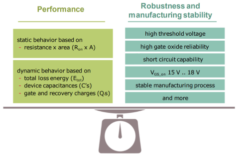
Advanced design activities are focusing on the field of specific on-resistance as the major benchmark parameter for a given technology. However, it is essential to find the right balance between the primary performance indicators like resistance and switching losses and the additional aspects relevant for actual power electronics designs, e.g. sufficient reliability
Login and learn how to determine the best design for your application

Read about how Silicon carbide (SiC) transistors are increasingly used in power converters, placing high demands on the size, weight and efficiency. The outstanding material properties of SiC enable the design of fast switching unipolar devices as opposed to bipolar IGBT devices. Thus, solutions which have been only possible in the low-voltage world (< 600 V), are now possible at higher voltages as well.
Login and read how CoolSiC™ MOSFETs revolutionize power conversion systems
CoolSiC™ schottky diodes
Infineon is the world’s first commercial Silicon Carbide (SiC) device supplier. Long market presence and experience enable Infineon to deliver highly reliable, industry-leading SiC performance. The differences in material properties between Silicon Carbide and Silicon limit the fabrication of practical Silicon unipolar diodes (Schottky diodes) to a range up to 100 V–150 V, with relatively high on-state resistance and leakage current. In SiC material Schottky diodes can reach a much higher breakdown voltage. The Infineon portfolio of Silicon Carbide (SiC) products covers 600 V and 650 V to 1200 V Schottky diodes.

CoolSiC™ hybrid devices
The combination of a Silicon-based switch and a CoolSiC™ schottky diode is called a “hybrid solution”.
Compared to Silicon IGBT solutions, the turn-on losses can be reduced. In addition higher switching frequency and higher current handling capability can be realized. Highest power density and efficiency can be achieved by using the chips as standalone components or in combination with silicon power devices in power modules. SiC diodes in particular are enabling parts to further extend the capabilities of IGBT technology.
| CoolSiC™ Hybrid Modules | CoolSiC™ Hybrid Discretes |
| The hybrid modules in the well-known EasyPACK™ come in booster as well as 3-level configuration. The portfolio consists of power modules where SiC diodes and IGBT chips form an ideal pair leveraging the best available performance in the targeted applications, such as solar energy systems. The number of power modules with SiC components will be complemented step by step with further parts, using either the combination of SiC diodes with silicon transistors or even SiC based transistors, currently based on the awarded CoolSiC™ technology. No matter the power of the application, our power module SiC portfolio enables a more efficient design, ranging from packages like EasyPACK™ 1B/2B to larger packages like EasyPACK™ 3B. |
CoolSiC™ Hybrid Discretes are a combination of two established, best-in-class semiconductor technologies: 650 V TRENCHSTOP™ 5 IGBTs and CoolSiC™ Schottky diodes G6. The resulting products have a performance similar to silicon carbide switches but come at an attractive price. |
FIT rates and gate-oxide reliability
In case of SiC to reduce FIT rates (quantifying hard fails) - two influencing factors must be considered:
- Cosmic ray effects (same as for Si devices)
- Gate oxide reliability (due to the oxide field stress)
Cosmic ray stability is usually achieved by optimizing the electric field distribution in the drift zone. However, to bring oxide FIT rates down, effective screening of electrically active defects is required. Principally, Si and SiC MOSFETs have pretty much the same intrinsic oxide lifetime as long as the devices do not contain defect-related impurities, i.e. extrinsic defects. SiC MOSFETs exhibit a much higher extrinsic defect density in the gate oxide, in contrast to Si MOSFETs. Devices with extrinsic defects break down earlier in comparison to defect-free devices. The challenge to guarantee sufficient reliability of the gate oxide of SiC MOSFETs is to reduce the number of devices being affected by extrinsics by means of electrical screening. Each device is subjected to a gate stress pattern - destroying those with critical extrinsics. As a consequence, the enabler for an efficient gate oxide screening is a nominal oxide thickness that is much higher than is typically needed to fulfill the intrinsic lifetime targets, what leads to a trade-off between gate-oxide-FIT-rate and device performance.

To further improve its SiC technology, Infineon invested a lot into testing on-state oxide reliability of electrically screened SiC MOSFETs and the off state oxide stress due to the electric field conditions in SiC power devices.
Today we can claim:
- Due to the optimized gate oxide thickness our gate oxide screening is more efficient compared to competing SiC MOSFET manufacturers.
- Lower gate oxide failure rates during the lifetime and no early failures translate into the highest possible gate oxide quality at the customer side.
SILTECTRA™ - innovative splitting technologies

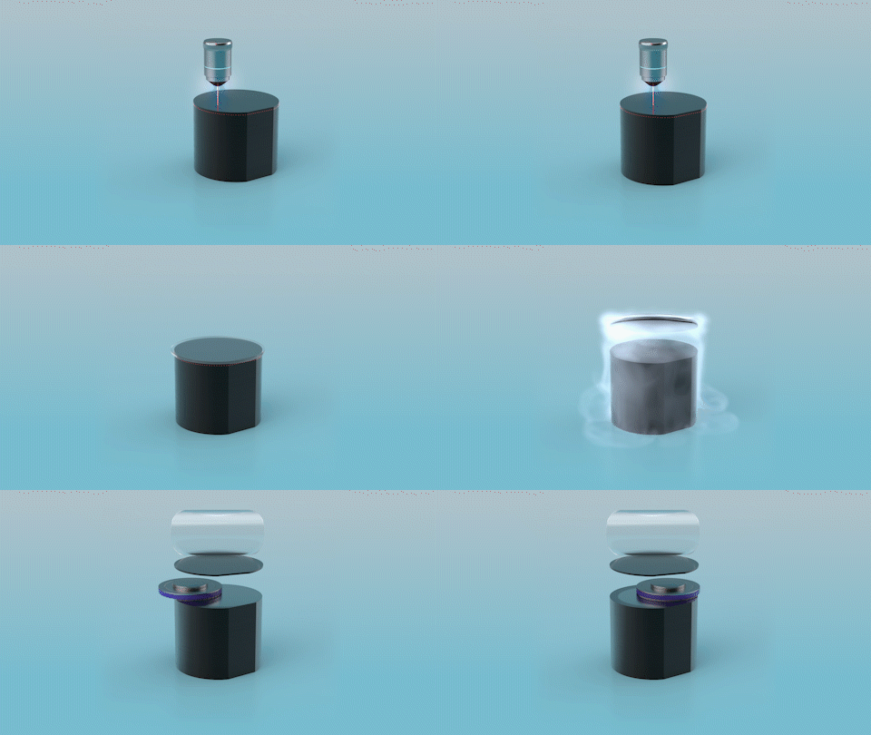
In 2018 Infineon acquired the Startup SILTECTRA™ to integrate innovative laser-based material separation technologies to the thin wafer technology competence. The SILTECTRA™ COLD SPLIT technology splits crystalline materials like Silicon Carbide with minimal loss of material compared to common sawing technologies.
Value proposition of SiC

For more than twenty years, Infineon has been at the forefront of developing solutions addressing demands for energy savings, size reduction, system integration and improved reliability in its products.
One of the most revolutionary developments was the use of SiC as a main compound in some of its devices.
Infineon is the world’s first SiC discrete power supplier.
It was the global pioneer in SiC technology and commercialization.
In this training we will present one of the most successful solutions that Infineon’s developed in this field.
Learn more about Value proposition of SiC here
