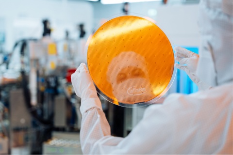
Ultra-thin Silicon Power Wafer Technology
Silicon ultra-thin wafers will help to significantly increase energy efficiency, power density and reliability in power conversion solutions in AI data center, consumer, motor control and computing applications. Halving the thickness of a wafer reduces the wafer’s substrate resistance by 50 percent, reducing power loss by more than 15 percent in power systems compared to solutions based on conventional silicon wafers of 40-60 micrometers thickness.
The ultra-thin wafer technology boosts the vertical power delivery design, which is based on the vertical Trench MOSFET technology allowing to reduce power losses and enhancing overall efficiency in power systems. Read more in this press release.

With only 20 micrometers thickness Infineon reached a breakthrough in processing the thinnest silicon power wafers ever manufactured on a diameter of 300 millimeter in a high-scale semiconductor fab. The wafers are thinner than human hair and half the thickness of current state-of-the-art wafers allowing Infineon to deliver outstanding customer value by pushing the technical boundaries of semiconductor technology.
The ultra-thin wafer technology marks a significant step forward in energy efficient power solutions and helps to leverage the full potential of the global trends decarbonization and digitalization. With this technological masterpiece, Infineon is solidifying our position as the industry’s innovation leader by mastering all three relevant semiconductor materials with Si, SiC and GaN.
CoolMOS™ - Revolutionary superjunction MOSFET families
OptiMOS™ - Innovation and performance for low and medium voltage power solutions
