OptiMOS™リニアFET
概要
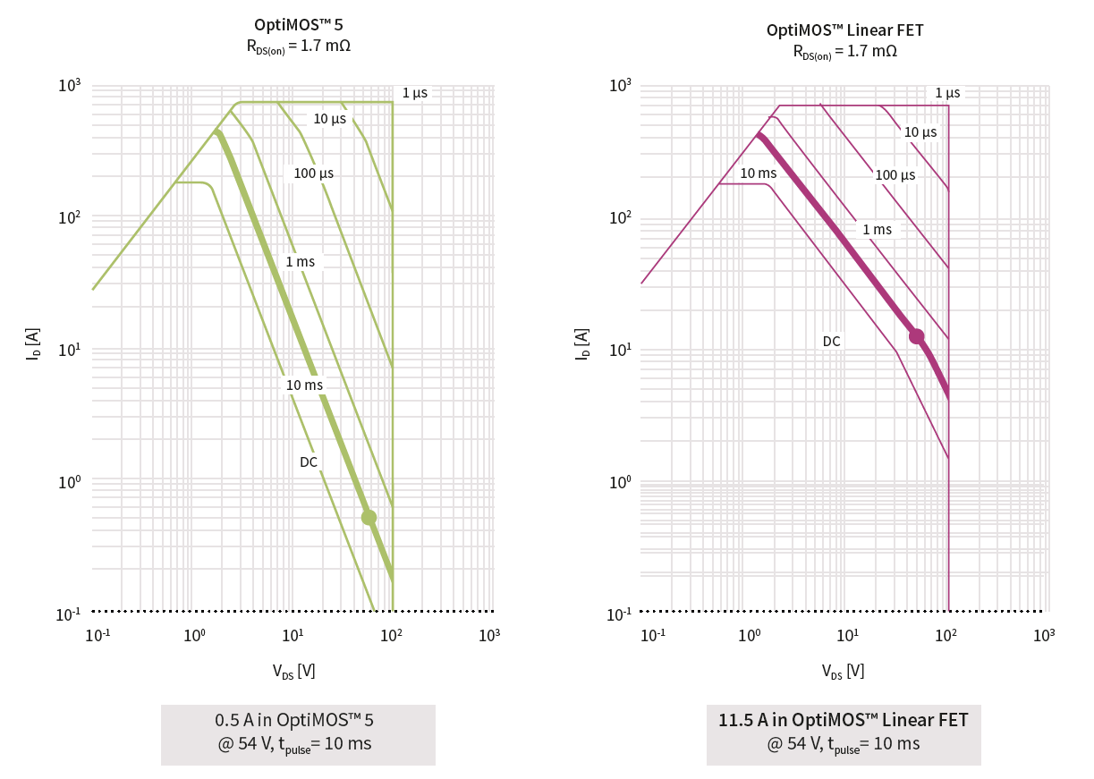
低オン抵抗RDS(on) と広い安全動作領域(SOA)を両立
OptiMOS™ Linear FETは、オン抵抗(R DS(on))とリニアモード性能とのトレードオフを回避する革新的な方式、すなわちエンハンストモードMOSFETの飽和領域での動作を可能にします。最新技術によるトレンチMOSFETのR DS(on) と、標準的なプレーナ型MOSFETの広い安全動作領域を両立しています。
この製品は、テレコムやバッテリ管理システムでよく使われるホットスワップやEヒューズアプリケーションに最適です。OptiMOS™ Linear FETは、高い突入電流を制限して、負荷の損傷を防止します。
- Wide safe operating area (SOA)
- Low RDS(on)
- High max. pulse current and continuous pulse current
- Multiple packages: D²PAK, D²PAK 7-pin, TOLL, PQFN 5x6 and 3.3x3.3
- Rugged linear mode operation
- Low conduction losses
- Higher in-rush current enabled for faster start-up and shorter down time
- Compatible footprint for drop-in replacement
- Telecom - hot-swap control
- Server - hot-swap control
- Battery management (BMS) – battery protection
- Power over ethernet (PoE) – port MOSFET
Complimentary products
製品
ハイライト


ビデオ
トレーニング


サポート